
Design center
Everything you need to put Harmony on a board: one application circuit, five layout rules, the land pattern, reliability data and the CAD files.
Type-B: the one circuit to remember
Put Harmony at the point of load with two 47 µF, 10 V capacitors in shunt with VOUT. That's the Type-B configuration, and it's the circuit TransSiP uses in almost every measurement on this site. Small-value capacitors are not needed.
Here is why it works. The two bulk capacitors create an anti-resonance near 1 MHz with S21 close to the noise floor. From that point upward, Harmony neutralizes the capacitors’ own inductance, so the rail stays on the noise floor out to multiple gigahertz.
The same three parts work on switchers, LDOs and PDNs, whatever the source and load impedance. What matters most is to give Harmony an anti-resonance at the frequency and depth of attenuation you need.
Shunt impedance, measured
| Frequency | Type-B | Dual Type-B |
|---|---|---|
| 1 MHz | 255.42 µΩ | 14.82 µΩ |
| 5 MHz | 141.34 µΩ | – |
| 14 MHz | – | 2.06 µΩ |
| 50 MHz | 104.24 µΩ | – |
| 100 MHz | 128.60 µΩ | 3.69 µΩ |
| 300 MHz | – | 4.55 µΩ |
| 1 GHz | – | 49.15 µΩ |
| 3 GHz | – | 252.52 µΩ |
Type-B values are from datasheet R009 §1.2, and dual Type-B values are from the Quick Start Guide §7. A typical PDN target impedance is 20 mΩ.
S21 of the Type-B board
| 900 kHz | −81.8 dB |
|---|---|
| 2 MHz | −99.5 dB At the VNA noise floor |
| 500 MHz | −97.5 dB At the VNA noise floor |
| 1.6 GHz | −80.6 dB |
| 6 GHz | −58.5 dB |
VNA marker readings, IF bandwidth 3.7 kHz (datasheet R009 §1.2). The readings marked at the VNA noise floor are limits of the instrument: Type-B’s true attenuation there is about −120 dB, below the noise floor of most instruments. Dual Type-B reaches −140 to −160 dB.
Three ways to place it
Type-B at the point of load
The default. One Harmony and two 47 µF capacitors where the rail meets its load. It gives broadband suppression from baseband to 6 GHz and isolates noise-sensitive circuits from noise-generating ones on a shared rail.
Dual Type-B to 20 GHz
Put one Type-B near the power source and a second at the point of load, inside the IC package or in the module. The dual configuration measured 62 dB of suppression at 10 GHz and 51 dB at 20 GHz, with 2 to 5 µΩ of shunt impedance from 14 MHz to 300 MHz.
SNJ conditioning at a switcher
For the best Switching Noise Jitter elimination, put Harmony pin 1 close to the power inductor and the feedback node, with traces as wide and as short as possible, and bulk capacitance at VOUT.
Switching regulators
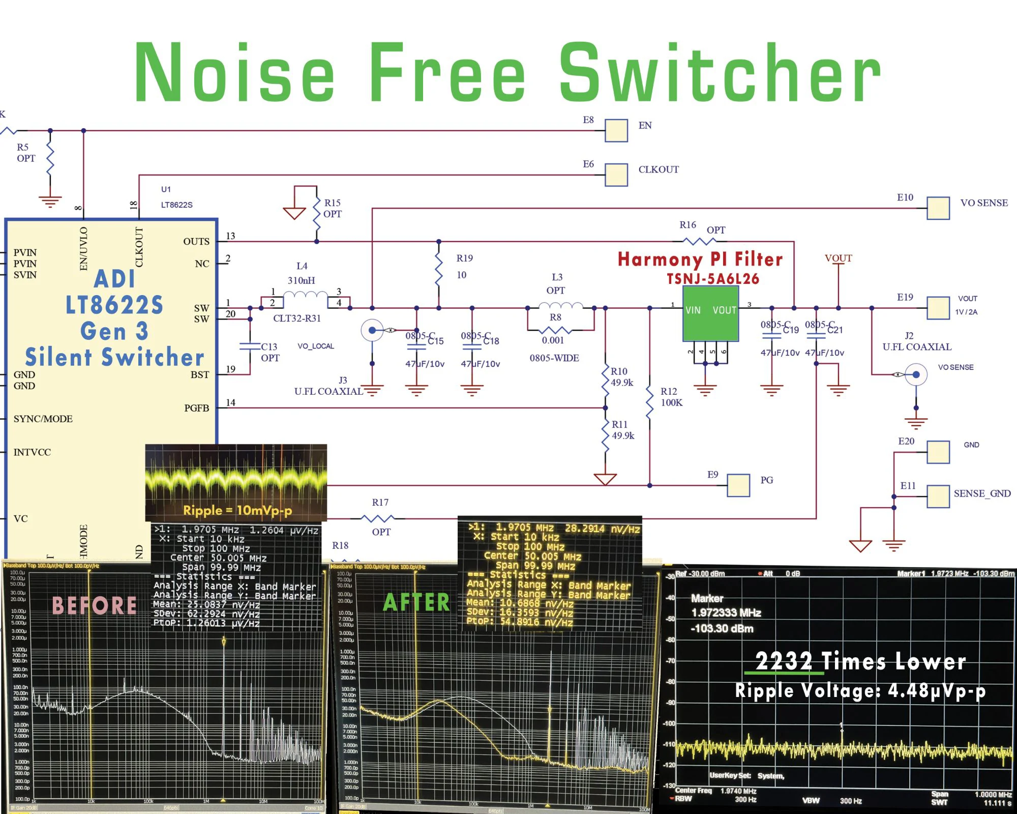
For DC-DC converters switching at 1 MHz or higher, Type-B typically brings ripple down to the microvolt range. That is at least 1,000 times lower than the best switchers available today, and a noise density of a few nV/√Hz. On an ADI LT8622S at 1 V and 2 A, ripple fell from 10 mVp-p to 4.48 µVp-p.
The lowest switching frequency with documented customer support is about 100 kHz. In that design, an LC pi filter of two 47 µF capacitors and a 2.2 µH inductor sits at Harmony’s VIN and sets the noise-floor starting point at about 100 kHz. That is not a lower limit for Harmony, just the lowest frequency implemented so far.
If a switcher radiates from its switch node or inductor, put the filter where the noise has to be gone: at the point of load. Our two-part Silent Switcher EMI video series shows the difference.
 Open a larger view
Ultra-low-noise LDOs
Harmony Type-B is deployed at an LDO’s VIN, at its VOUT, and at its voltage or current reference node where there is one. It has been used with the LT3046, ADM7150, LT3045 and TPS7A94, and it takes noise suppression beyond the LDO’s own capability under real operating conditions.
- VIN: keeps upstream switching noise from reaching the regulator.
- VOUT: takes the output to the noise floor, beyond what the LDO’s own PSRR can reach at high frequency.
- Reference node (LT3045 SET pin): replace the conventional CSET with Harmony and bulk capacitors. This gives typically less than 100 µΩ of shunt impedance from 1 MHz to 1 GHz across the set resistor. Use smaller bulk capacitors here if start-up time matters.
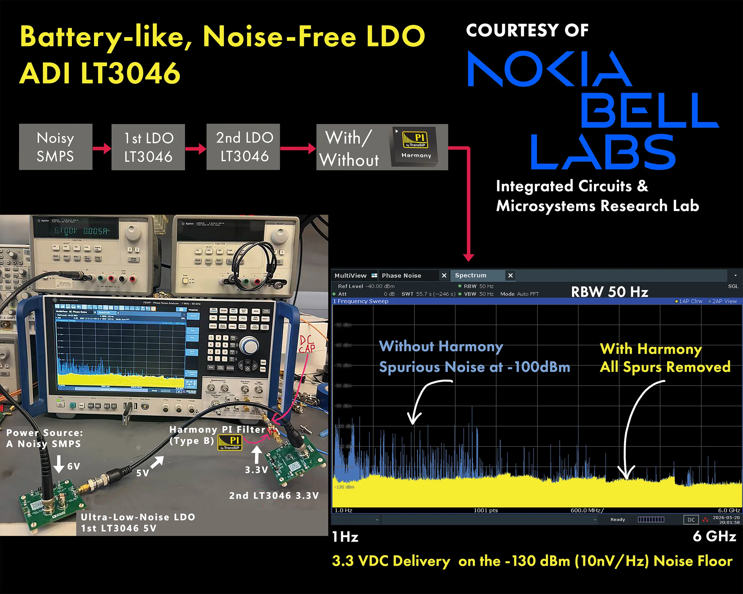
Newest, from Nokia Bell Labs: two ADI LT3046 LDOs in series still left spurs at about −100 dBm on a rail fed by a noisy switcher. With Type-B after the second LT3046, every spur was removed and the 3.3 V rail sat on the −130 dBm (10 nV/√Hz) floor from 1 Hz to 6 GHz.
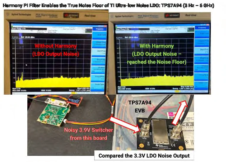
In earlier measurements with Nokia Bell Labs, a TI TPS7A94 fed from a noisy 3.9 V switcher reached the spectrum analyzer’s noise floor from 3 Hz to 6 GHz once Type-B was added at its output.
 Open a larger view
 Open a larger view
Clocks: VCO, VCXO, TCXO, VCTCXO
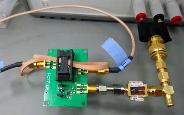
To evaluate, connect the Harmony Type-B evaluation board between the noisy supply and the clock’s VCC with SMA cables. In the 122.88 MHz VCXO test, RMS jitter from a noisy 3.3 V rail fell from 233 fs to 20 fs, against 18 fs from the cleanest lab supply.
In production, put Type-B on the oscillator and PLL supplies, and between the PA or digital rails and the LO chain.
Layout rules
Harmony’s performance depends on its ground connection. Imagine the layout running at 6 GHz.
- Ground planePut a ground plane on the inner layer directly under Harmony. Connect each GND terminal to it with 0.2 mm (8 mil) vias placed right next to the terminal, at least one at each end. Do not use long traces or thermal reliefs. Connect the plane to the battery or source with the widest, shortest path you can.
- Via-in-padFor compact designs, via-in-pad on all GND terminals is highly recommended.
- Laser viasLaser vias are typically 100 µm or smaller, so place many of them in each GND terminal rather than a few.
- Keep VIN and VOUT apartDo not overlap VIN and VOUT traces or power planes on vertically adjacent layers. Overlap couples the noise on VIN into VOUT.
- Stitching viasTie the ground planes of every layer together with many closely spaced vias around Harmony’s GND terminals. This keeps ground inductance low across at least 6 GHz.
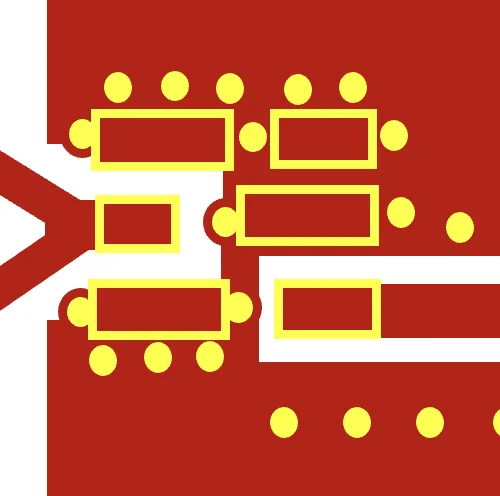
Stitch ground generously
Many vias around Harmony’s GND terminals keep the ground low-impedance across multiple gigahertz.
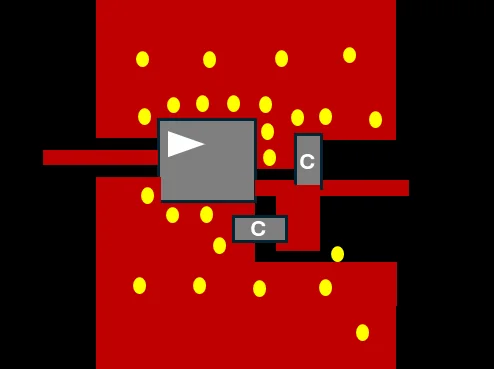
Return capacitor ground to Harmony
A shared return couples high-frequency noise from about 1.6 GHz upward.
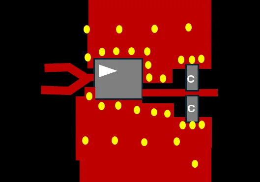
Ground capacitors to the plane, extend VOUT
This is the most effective connection from 1.6 GHz to 6 GHz. An extra 5 to 8 mm of VOUT adds 5 to 10 dB from 3 GHz to 6 GHz.
Layout drawings from the Harmony PCB Layout Guideline 25V3 and the LT3045 application note.
Land pattern and pinout
Pin assignment
| Pin | Name | Function |
|---|---|---|
| 1 | VIN | Voltage or signal input |
| 2 | GND | Ground |
| 3 | VOUT | Voltage or signal output |
| 4 | GND | Ground |
| 5 | GND | Ground |
| 6 | GND | Ground |
Package and marking
| Package | LGA-2226, 2.60 × 2.20 mm (±0.05), 0.9 mm max height |
|---|---|
| Marking | ▶ TSNJ, date code A4WW, TransSiP A = year (2026), 4 = run group, WW = week number |
| Reel | 3,000 per 180 mm reel, 8 mm tape, pin 1 in Q2 |
| Assembly | MSL 2a, lead-free reflow per J-STD-020 |
Reliability
18.1 FIT at 3.3 V and 45 °C, an MTTF of about 6,300 years.
500 parts, 1,000 hours at 85 °C with 4 V on VIN and VOUT. Zero failures. JIS C5003, 60% confidence. Voltage exponent 6, temperature doubling every 8 °C. 1,834 FIT at the stress condition.
Calculated FIT and MTTF values are estimates, not guarantees. Report TSQA2407-TSNJ-MTTF, 8 July 2024.
| Operating voltage at 25 °C | FIT (failures per 10⁹ h) | MTTF (years) |
|---|---|---|
| 0.5 V | 0.000039 | 2.95 billion |
| 1 V | 0.0025 | 46.2 million |
| 2 V | 0.158 | 721,110 |
| 3.3 V | 3.19 | 35,735 |
| 4 V | 10.1 | 11,267 |
| 5 V | 38.6 | 2,954 |
| 6 V | 115.4 | 989 |
The predicted failure rate rises steeply toward the 6 V maximum, so we recommend voltage derating for long-term reliability.
CAD and documents
The datasheet downloads directly. Everything else comes in the Harmony Materials Package, which we email on request.
Datasheet
- Harmony PI Filter datasheet, Rev 9PDF, 14 pages, March 2026 Download
Getting started
CAD models
Layout
- PCB layout guideline: grounding and bulk-capacitor placementPDF, rev 25V3 Request
Application notes
Case studies
- TransSiP Noise Free Innovations: application examplesPDF, 23 pages, rev 26V2 Request
Quality and compliance
- RoHS 3 certificate of compliancePDF, TSQA-RoHS3 Download
- EU REACH certificate of compliancePDF, 13 pages, TSQA-REACH, February 2026 Download
- Halogen-free certificate (IEC 61249-2-21)PDF, TSQA-HF Download
- TSNJ-5A6L26 reliability qualification (RTV program)PDF, 3 pages, TSQA-TSNJ-RTV Download
- TSNJ-5A6L26 FIT and MTTF predictionPDF, 2 pages, TSQA2407, July 2024 Download
"Request" items ship together in the Harmony Materials Package. One request covers all of them, and we send the package to your work email.