
The quietest switcher on the bench
The ADI LT8622S is a third-generation Silent Switcher. It is one of the lowest-noise switching regulators you can buy. ADI specifies 4 µVRMS of output noise from 10 Hz to 100 kHz and 4 nV/√Hz of spot noise at 10 kHz. It switches anywhere from 300 kHz to 6 MHz and delivers 2 A (the LT8624S delivers 4 A).
Those figures are accurate, and they stop at 100 kHz. Anything a fast switch node produces above that band shows up as “ripple”. How much ripple you measure depends on the bandwidth of the instrument you measure it with.
Same rail, two oscilloscopes
We ran an LT8622S at a 2 MHz switching frequency and measured its output on two oscilloscopes.
| Instrument | Bandwidth | Sample rate | Ripple measured |
|---|---|---|---|
| Tektronix TDS7154B | 1.5 GHz | 20 GS/s | 4 mVp-p |
| Keysight Infiniium MXR B-Series | 6 GHz | 16 GS/s | 10 mVp-p |
The board and the rail were the same, yet the 6 GHz instrument shows two and a half times the ripple. The difference is RF and microwave content that rides on the ripple. A 2 MHz switch edge has harmonics and edge-related spurs that reach well past 1.5 GHz, and a slower instrument simply never sees them.
That matters because ripple is usually quoted with a 20 MHz bandwidth limit, the long-standing convention for power supply measurements. A 20 MHz number is fine for a digital core that only cares about DC accuracy. It says nothing useful about a PLL, an LNA, a SerDes lane or a 5G transceiver, because those loads are most sensitive in exactly the band the limit throws away.
Adding one Harmony PI Filter
Next we placed a single TSNJ-5A6L26 between the regulator and the load, and watched the same rail on the MXR.
- The 2 MHz fundamental fell from about −59 dBm to about −97 dBm. That is a 38 dB reduction, close to 100× in voltage.
- Harmonics of the switching frequency were eliminated.
- High-frequency and microwave spurs were eliminated as well.
It helps to put those spectrum readings into volts. In a 50 Ω system:
VRMS = √(50 Ω × P) so −97 dBm = 2.0 × 10⁻¹³ W → 3.2 µVRMS → 8.9 µVp-p for a sine
The starting tone, −59 dBm, is about 250 µVRMS, or 0.7 mVp-p. After Harmony, all that remains on the rail is a single 2 MHz tone of about 9 µVp-p. A low-frequency tone that small does not disturb the VCXOs, TCXOs, LNAs and PAs that the rail feeds.
The 2025 follow-up: Type-B at 1 V and 2 A
In 2025 we repeated the experiment on the LT8622S evaluation board using the Type-B configuration: Harmony plus two 47 µF, 10 V 0805 capacitors at VOUT, with the regulator delivering 1 V at 2 A.
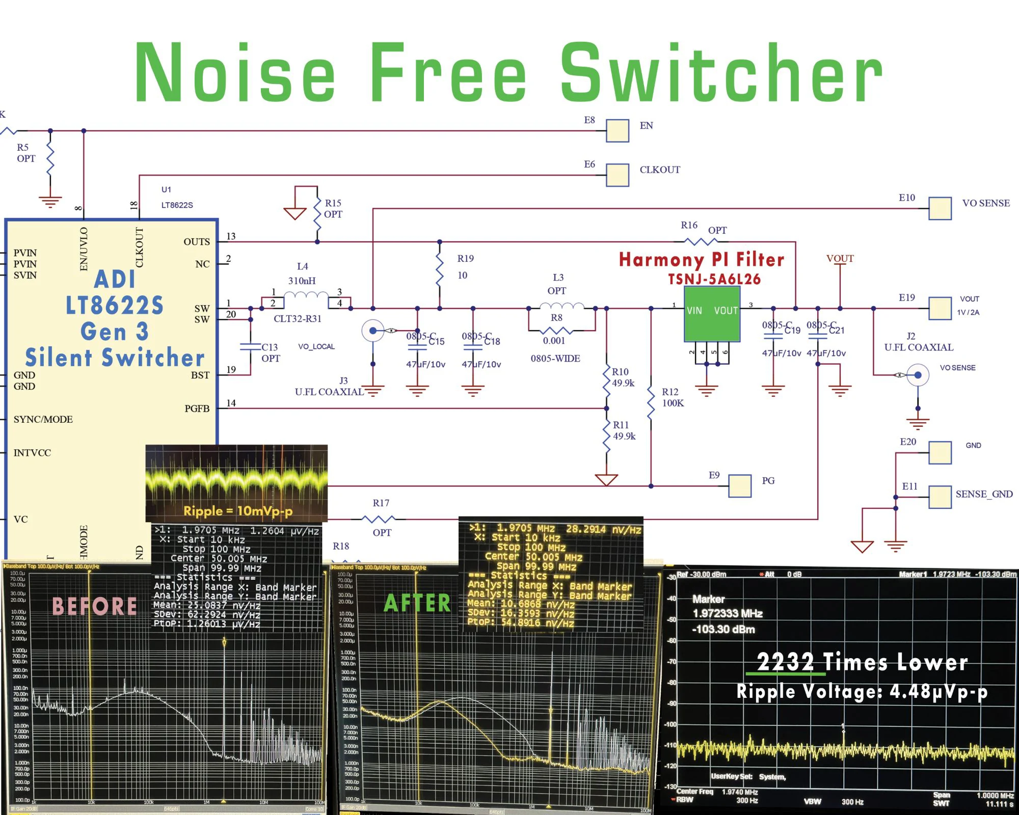
| Measurement | Without Harmony | With Harmony Type-B |
|---|---|---|
| Output ripple | 10 mVp-p | 4.48 µVp-p |
| Switching fundamental (1.97 MHz) | 1.26 µV/√Hz | 28.3 nV/√Hz, −103.3 dBm |
| Mean noise density, 10 kHz to 100 MHz | 25.1 nV/√Hz | 10.7 nV/√Hz |
Ripple is 2,232 times lower. The broadband noise floor falls too, by more than half, which confirms what the Quick Start Guide describes. Harmony removes the switching harmonics and spurs, and it also reveals headroom below the regulator’s own system noise floor.
The real noise floor sits 20 dB below the datasheet
Harmony’s result is not limited by how many decibels of suppression it adds. Once the switching noise is gone, what is left is the true intrinsic noise floor of the power source itself. On the LT8622S, that floor measured 20 dB lower than the ADI datasheet shows. A Silent Switcher is quieter than even its own datasheet reveals, and Harmony is what lets you see it.
Where the filter goes matters
In January 2026 we published a second pair of measurements on the LT8622S and LT8624S. These looked at radiated EMI. Silent Switchers can still radiate from the switch-node surface and the power inductor, and the question was where a filter does the most good.
- Harmony right next to the inductor. Part of the radiated energy bypasses the filter and couples into the VOUT trace downstream of it.
- One Harmony at the point of load. We removed the filter at the inductor and placed a single Harmony where the rail arrives at its load. The rail came back to the Silent Switcher’s own noise floor, and even lower, despite the radiated energy it picked up along the way.
This is exactly how we recommend placing Harmony. Put pin 1 close to the power inductor and the feedback node to condition Switching Noise Jitter inside the regulator’s loop. When a rail travels across the board and collects radiated energy on the way, the filter does its best work where the noise has to be gone, which is at the load. If you are not sure which case applies to your layout, the evaluation board lets you measure both.
What to take into your next design
- Measure ripple at the bandwidth your loads care about. If your most sensitive load operates at 6 GHz, a ripple figure limited to 20 MHz tells you nothing about it.
- Think in decibels and volts together. Every 20 dB is a factor of 10 in voltage, so −59 to −97 dBm is roughly 100×.
- Let the switcher feed sensitive loads directly. With Harmony at the output you keep the switcher’s efficiency. You no longer need an LDO post-regulator and its dropout loss.
- Place the filter for the noise you are fighting. Put it near the inductor and FB node to condition SNJ in the loop. Put it at the point of load when the rail picks up radiated energy on its way.
- Ground it properly. Put a ground plane directly under the part and a 0.2 mm via at each GND terminal. Do not use thermal reliefs. Use via-in-pad. All six of our layout rules are in the datasheet.
Sources
- TransSiP PI Series, part 1: Infiniium MXR B-Series and ADI Silent Switcher LT8622S switching noise (video)
- TransSiP PI Series, part 2: ADI Silent Switcher LT8622S becomes noise-free (video)
- Silent Switcher EMI, part 1: why filter placement matters (video)
- Silent Switcher EMI, part 2: a single filter at the point of load (video)
- TransSiP, ADI LT8622S Noise Free Silent Switcher poster (2025), Harmony Materials Package
- Analog Devices, LT8622S product page and data sheet
- TransSiP, Harmony PI Filter datasheet TSNJ-DS-R009, Rev 9