
A lab-grade clock meets a real-world supply
Rakon builds oscillators for reference clocks, one of the parts every radio system depends on. As 5G spectrum widened, Rakon designed a very low-noise oscillator to meet the tighter phase-noise requirements of 5G. It then ran into a problem that sits outside the oscillator: the quality of the power supply.
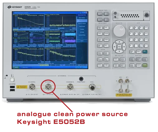
In the lab, oscillators and 5G chipsets are characterized from a very clean DC bias. Instruments that can supply one cost from more than $2,000 to hundreds of thousands of dollars in the case of a signal source analyzer such as the Keysight E5052B. Handsets and base stations ship with ordinary switching supplies instead. The clock that met its specification on the bench then misses it in the product.
The experiment
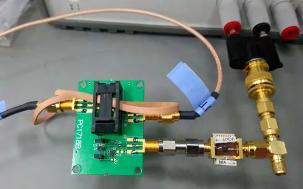
TransSiP and Rakon tried a simple topology: a noisy SMPS, then a Harmony PI Filter, then the 5G reference oscillator. It is the “eliminate the DC-DC effect for ultra-low phase noise” example in the Harmony datasheet.

With the Harmony filter in place, and still running from the noisy supply, the reference clock’s phase noise improved by about six times. In a 5G transceiver, that corresponds to up to 15 dB more SNR at the RF ADC. We are now working with a 5G lab and a national institute to measure the effect at system level.
From supply noise to phase noise
An oscillator’s frequency depends slightly on its supply voltage. Datasheets call this frequency pushing. Any noise on the supply therefore modulates the frequency:
- Switching ripple at the regulator’s fundamental and its harmonics appears as discrete spurs at those offsets.
- Broadband supply noise raises the phase-noise floor across the offsets it covers.
- Switching Noise Jitter, switching noise whose phase moves in time, smears those spurs so they are hard to isolate and hard to filter in the frequency domain alone.
Integrate the phase noise over the band that matters and you get the clock’s rms jitter. ADI’s MT-008 tutorial walks through that integration.
From jitter to SNR
For a converter that samples a full-scale signal at frequency fin, clock jitter σt sets an upper limit on SNR:
SNRjitter = −20 · log10(2π · fin · σt)
The formula is ruthless at RF. At 3.5 GHz, in the middle of 5G band n78 (3.3 to 3.8 GHz):
| RMS jitter | Jitter-limited SNR at 3.5 GHz |
|---|---|
| 100 fs | 53.2 dB |
| 50 fs | 59.2 dB |
| 16.7 fs | 68.7 dB |
Cutting jitter six times, from 100 fs to 16.7 fs, adds 20·log10(6) ≈ 15.6 dB. That matches the 15 dB TransSiP measured. The match holds if “six times” refers to rms jitter, and if the receiver is jitter-limited. Direct-RF sampling receivers usually are.
Measured: a 122.88 MHz VCXO on a noisy 3.3 V rail
TransSiP then measured the effect directly. A 122.88 MHz VCXO, the reference frequency used throughout 5G, ran from a noisy 3.3 V PDN, the way it does in real equipment. RMS jitter was integrated from 12 kHz to 20 MHz on a Keysight E5052B.
| Supply | RMS jitter | Jitter-limited SNR gain (any input frequency) |
|---|---|---|
| Noisy 3.3 V PDN, typical of real 5G equipment | 233 fs | Reference |
| Same PDN + Harmony (first demo board) | 32 fs | +17.2 dB |
| Same PDN + Harmony Type-B (optimized) | 20 fs | +21.3 dB |
| Lab ideal: E5052B clean bias | 18 fs | +22.2 dB |
With Type-B, the noisy rail came within 2 fs of the cleanest bias a lab can provide.
The same holds for a differential crystal oscillator of the kind used in data-center links. With a deliberate 200 mVp-p signal injected on its supply, phase noise with Harmony was 29.6 dB better at 20 kHz offset, 22.2 dB better at 100 kHz, and 18.3 dB better at 1 MHz.
What this means for radio teams
- A commodity supply can deliver a lab-grade bias. The point of the experiment is that an ordinary switching supply, filtered by Harmony, can match the bias quality that used to require a laboratory instrument.
- Filter the oscillator and PLL rails. Put Harmony Type-B on the oscillator and PLL supplies. Isolate the clock from the PA and digital loads with a filter between them.
- Characterize with your real supply. When you measure phase noise, power the oscillator from your product’s own supply as well as from the analyzer’s clean bias. The gap between those two measurements is the performance you are shipping.
Sources
- TransSiP, Wireless benefits: making waves in the 5G ecosystem
- Analog Devices, MT-008 tutorial: Converting Oscillator Phase Noise to Time Jitter
- TransSiP, Harmony PI Filter datasheet TSNJ-DS-R009, Rev 9 (application examples, section 1.3)
- TransSiP, Noise Free ULPN 122.88 MHz VCXO 25V1, and Harmony Quick Start Guide 25V3 §9 (Harmony Materials Package)
- TransSiP, Noise Free Innovations 26V2, p. 9: power-supply phase-noise test (Harmony Materials Package)